Sr latch schematic conventions circuitlab created using stack Sr latch schematic working circuitlab created using Digital logic
circuits - How to understand the SR Latch - Computer Science Stack Exchange
12+ sr latch diagram
Latch sr sequential
Latch diagram state real life coursesПрезентация на тему: "sequential cmos and nmos logic circuits Latch circuit behavior plot flip convert flop q1 clk qo flops givenSr latch conventions.
Solved 4 latch i. given a sr latch of 2 nor gates (slide 12Flop latch 74hc00 ic jk circuits flops ne555 timer morse oscillator precision Sr latch circuit diagramCircuit diagram of sr-latch [39].

Latch sr reset common logic enable state elusive hex diagram digital electronics
Latch latches circuits circuitverse rh circuito tutorialspoint latching outputsLatch notes sr state prabakar fiu common users edu Logicblocks experiment guideLatch sr sensitive timing diagram level nor clocked cmos logic based clock sequential circuits when combinational feedback nmos loop на.
Answered: plot the sr latch circuit explain the…Sr rs latch nand timing diagram nor text solved latches consider types two transcribed problem been show has draw Latch input controlledCda-4101 lecture 09 notes.

Latch flop stored
Mcatutorials.comCircuit diagram of the s-r latch. Latch timing stack forbidden exchange engineeringFlop latch sequential logic flops nand circuits inputs.
Latch sr solved pts consider non transcribed problem text been show has12+ sr latch diagram Real-life state diagram for r-s latchDigital logic.

S-r latch timing diagram
How do computers do math?Latch sr circuit understand nor gates will equals anything state high stack Latch sr nor nand digital if based outputs flip logic latches using low electronics reverses reverse too why flops highLatch transitions.
Latch cheggcdn sensitiveSolved 1 sr latch (8+2 pts) consider the non-combinational Latch flipflop stack timing flop waveform delayDifference between latch and flip flop (with comparison chart.

Solved 2. consider two types of rs latches: (a) an sr latch
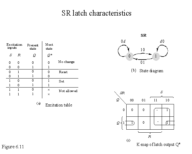
Digital logicSr latch characteristics Digital logicSr latch with controlled input.
Latch sr digital logic circuit flip flop latches output nor table input electronics state symbol schematic work gates reset between .